From 2024 to 2025, the advanced packaging market reinforced its strategic role across markets. Once confined to specific high-end applications, it is now a pillar of mass adoption in consumer electronics and an enabler of emerging markets, including AR/VR, Edge AI, aerospace, and defence.
At the same time, the telecom and infrastructure segment is experiencing unprecedented growth, with a 14.9% increase between 2024 and 2030, making it the segment with the highest growth. This momentum is powered by AI accelerators, GPUs, Cloud and data centre demand, and chiplet-based architectures. As system complexity rises, advanced packaging technologies such as CoWoS, SoIC, EMIB, I-Cube, and 3D stacking provide the performance and integration levels required by hyperscale infrastructure players.
“Advanced packaging has reinforced its role as a cornerstone within the semiconductor value chain, reshaping not only mass markets but also highly sensitive domains. Its trajectory reflects a portfolio expansion designed to enable a wide spectrum of industries,” said Bilal Hachemi, Senior Technology & Market Analyst, Semiconductor Packaging at Yole Group.

Players, investments, and regional strategies in the advanced packaging industry
The 2024 ranking of advanced packaging players highlights a shifting landscape: IDMs dominate with Intel, Sony, Samsung, YMTC, and SK Hynix leading, followed by OSATs and foundries such as TSMC. Memory players and diversified portfolios have reshaped the Top 10.
This reshaping has been enabled by a wave of unprecedented investments:
- TSMC ramped CoWoS capacity after acquiring a facility from Innolux in Taiwan and is also scaling SoIC
- ASE, Amkor, and Intel boosted US capacity in line with CHIPS Act incentives, aligning with customer needs from NVIDIA and Apple
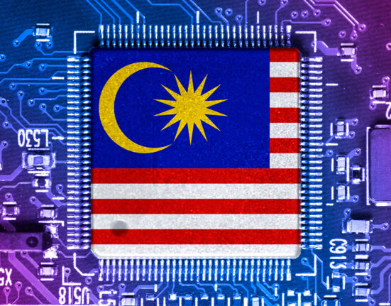
- Unisem and MPI expanded in Malaysia and Vietnam to avoid China-Taiwan tensions and reduce logistics costs
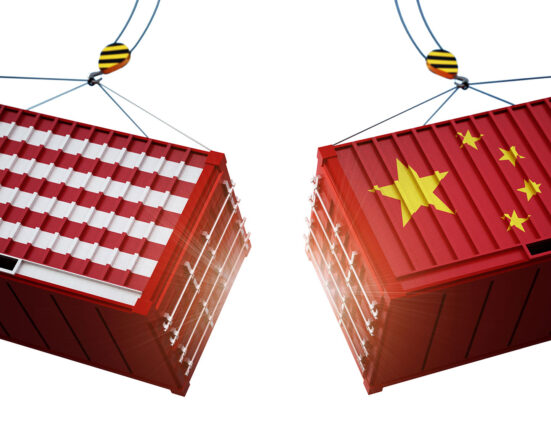
- Forehope, Lingsen, and ChipMOS reinforced their strong mainland China positions, investing heavily in automation and customer clustering
- JCET announced a $1.5 billion investment to strengthen domestic AP capabilities
- In Nanjing, HT-Tech launched a second-phase expansion worth 10 billion yuan, about $1.4 billion
- Tongfu Microelectronics announced a 7.5 billion yuan (~$1.0 billion) advanced packaging project targeting flip-chip, multi-layer stacking, WLP, and PLP, with completion planned by 2029
- Across Jiangsu, Hubei, and other regions, at least seven new advanced packaging fabs are under construction in China, signalling a long-term push for independence and capacity scaling
What’s next?
“We are witnessing the start of a new cycle for advanced packaging. Market leaders are reshaping their strategies with major investments and alliances to secure growth across consumer, AI, and infrastructure markets,” states Hachemi.

For example, collaboration has become a defining factor for advanced packaging success. Overflow partnerships between TSMC, ASE, and Amkor, Intel’s EMIB assembly collaboration with Amkor, and regional consortia highlight the necessity of shared innovation. And for disruptive technologies such as CPO, robust collaboration is essential to overcome material and equipment barriers. The supply chain is moving toward resilient, regionalised, and vertically integrated ecosystems, reducing reliance on global volume-centric sourcing.
With revenues expected to reach $79.4 billion by 2030, advanced packaging is no longer an optional innovation; it is the foundation of semiconductor growth. From smartphones to data centres, from AI accelerators to defence systems, advanced packaging is positioning itself as the enabling force behind the industry’s transformation, and Yole Group’s analysts will continue their investigation to deliver up-to-date and accurate analyses of this industry week after week.