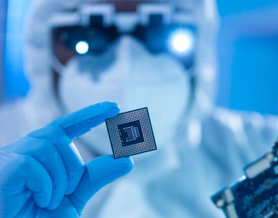
Semiconductors are at the heart of modern electronics, powering everything from smartphones and computers to electric vehicles and industrial machinery.
Their production involves a highly sophisticated process that combines chemistry, physics, and engineering to create intricate devices capable of controlling electrical signals. Understanding how semiconductors are made provides insight into one of the most critical components of today’s technology landscape.
Raw materials: silicon and beyond
The primary material used in semiconductor manufacturing is silicon, which is derived from sand. Silicon is preferred because it is abundant, cost-effective, and possesses ideal electrical properties for controlling electrical conductivity. The process begins by extracting and purifying silicon to achieve a highly refined form known as electronic-grade silicon.
For more advanced semiconductors, other materials such as gallium arsenide (GaAs), silicon carbide (SiC), and indium phosphide (InP) are used. These materials offer unique properties, such as higher thermal conductivity or faster electron mobility, which make them suitable for specialised applications like power electronics and telecommunications.
The wafer production process
Once the raw material is prepared, the next step is to produce a silicon wafer a thin, circular slice of silicon that serves as the foundation for semiconductor devices.
Crystal growth
Silicon ingots, large cylindrical crystals, are grown using the Czochralski process. In this method, a small seed crystal is dipped into molten silicon, then slowly rotated and pulled upwards. This controlled process results in a single crystal structure with minimal defects.
Wafer slicing
The silicon ingot is sliced into thin wafers using diamond-tipped saws. These wafers are typically around 200 to 300 mm in diameter, with newer processes moving towards even larger sizes to increase production efficiency.
Wafer polishing
After slicing, the wafers are polished to achieve a mirror-like finish, ensuring a flat and smooth surface. Any imperfections on the wafer can affect the performance of the final semiconductor device.
Photolithography: the blueprint for semiconductors
Photolithography is a key step in semiconductor manufacturing that defines the patterns and circuits on the wafer. This process involves several steps:
Cleaning
The wafer is thoroughly cleaned to remove any contaminants that could interfere with the subsequent steps.
Photoresist application
A light-sensitive material called photoresist is applied to the wafer. The thickness and composition of the photoresist are carefully controlled to achieve the desired resolution.
Mask alignment and exposure
A photomask, which contains the circuit design, is aligned with the wafer. The wafer is then exposed to ultraviolet (UV) light, which transfers the pattern from the mask onto the photoresist.
Developing
The exposed photoresist is developed, revealing the underlying pattern on the wafer. This pattern serves as a guide for the subsequent etching process.
Etching and doping: creating functional layers
After photolithography, the wafer undergoes etching and doping processes to create the various layers and regions that form the semiconductor device.
Etching
Etching removes unwanted material from the wafer to create the desired structures. It can be performed using:
- Wet etching: Involves chemical solutions to dissolve the material.
- Dry etching: Uses plasma or reactive gases to achieve more precise results.
Doping
Doping is the process of introducing impurities into the silicon to modify its electrical properties. This step is crucial for creating the p-type and n-type regions that enable semiconductor devices to control electrical current.
Metalisation and packaging: finalising the semiconductor
Once the wafer is patterned, etched, and doped, it is ready for metalisation the process of adding conductive materials to form electrical connections.
Metalisation
Thin layers of metal, such as aluminium or copper, are deposited on the wafer to create the interconnections between different components on the chip. This step is essential for ensuring the semiconductor can interact with external circuits.
Packaging
After the individual chips are created on the wafer, they are cut, tested, and enclosed in protective packaging. Packaging provides mechanical protection, heat dissipation, and electrical connections to the outside world.
Testing and quality control
Each semiconductor chip undergoes rigorous testing to ensure it meets performance specifications. These tests check for electrical properties, functionality, and reliability under various conditions. Chips that pass the tests are marked as functional and are ready for integration into electronic devices.
The role of advanced manufacturing techniques
Modern semiconductor manufacturing incorporates advanced techniques to improve efficiency and performance. Some of these include:
- Extreme Ultraviolet (EUV) Lithography: A cutting-edge photolithography technique that allows for the creation of smaller and more complex features on chips.
- 3D Packaging: Stacking multiple semiconductor layers to increase performance and reduce size.
- Chemical Mechanical Polishing (CMP): Ensuring flat surfaces between layers to improve chip reliability.
Conclusion
The semiconductor manufacturing process is a complex interplay of materials science, engineering, and precision manufacturing. From raw silicon to highly integrated chips, each step requires meticulous attention to detail to achieve the desired performance and reliability. As technology advances, semiconductor manufacturing continues to evolve, enabling the development of faster, more efficient, and more powerful electronic devices that drive innovation across industries.


