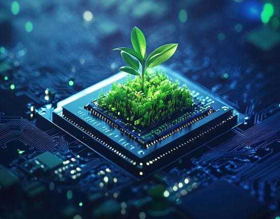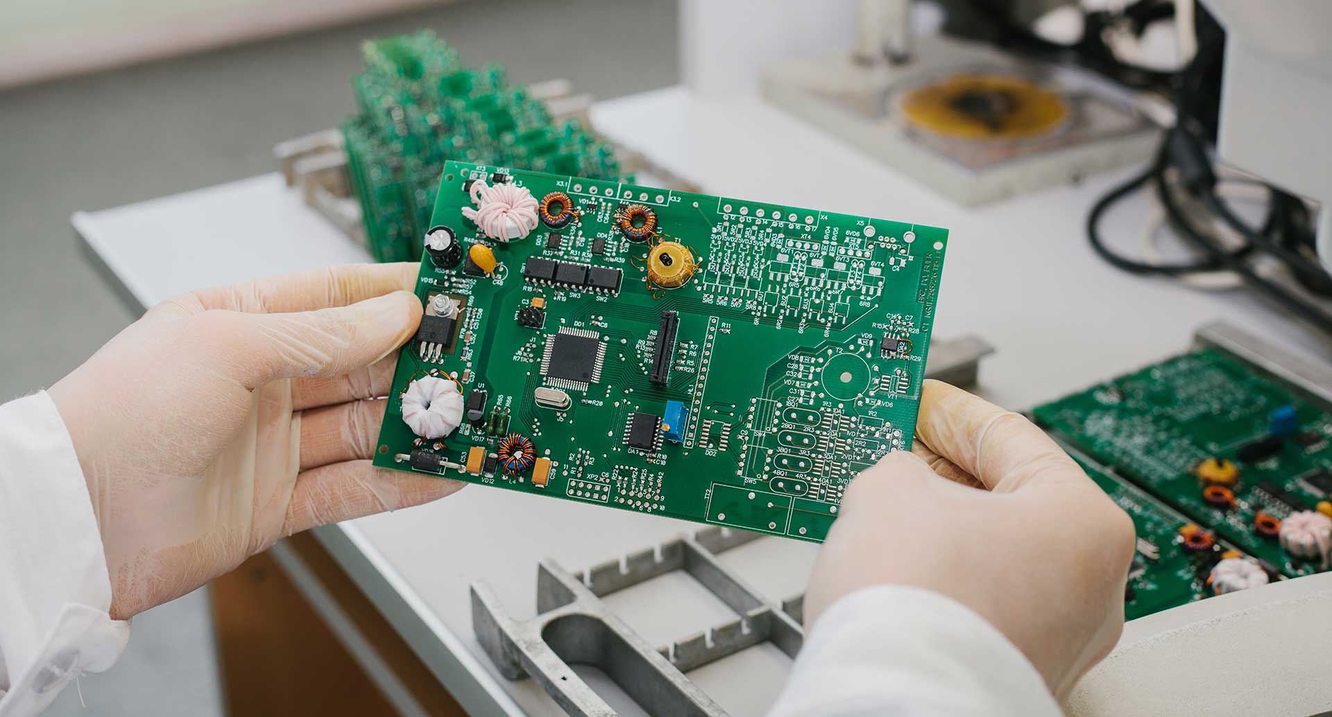
Electronics are everywhere. From consumer devices to industrial equipment, printed circuit boards (PCBs) form the core of modern technology. As demand for electronics grows, so does their environmental impact. Designers face a new challenge: creating functional, efficient PCBs while reducing environmental harm.
Sustainable PCB design goes beyond recycling or reducing waste. It considers the full life cycle of the product. Each material, process, and design decision contributes to the overall environmental footprint. Integrating life cycle analysis (LCA) into PCB design allows engineers to make informed, environmentally conscious decisions.
What is Life Cycle Analysis (LCA)?
Life Cycle Analysis, or LCA, evaluates the environmental impact of a product throughout its life. It tracks each stage, from raw material extraction to disposal or recycling. LCA measures energy use, emissions, and waste, giving designers a complete picture of environmental effects.
Sidebar: LCA vs. traditional environmental assessment
Traditional assessments often focus on a single stage, like manufacturing or disposal. LCA, in contrast, evaluates the entire life cycle. This approach identifies hidden impacts and highlights opportunities for improvement.
Key LCA stages include:
- Raw Material Extraction – mining and processing metals, plastics, and chemicals
- Manufacturing – PCB fabrication, assembly, and testing
- Distribution – packaging, shipping, and logistics
- Use Phase – energy consumption and reliability during operation
- End-of-Life – disposal, recycling, or recovery of materials
Each stage carries environmental costs. Copper mining consumes water and energy. PCB fabrication can release volatile organic compounds (VOCs). Transportation contributes to carbon emissions. Disposal can generate hazardous waste. LCA quantifies these effects, helping designers make better choices.
Some designers, such as those at HyePeak, apply LCA principles in PCB design to reduce environmental impact.
Applying LCA to PCB design
Integrating LCA begins with material selection. Designers must balance environmental performance with electrical requirements. Choosing recyclable or low-impact substrates can significantly reduce environmental harm. Lead-free solder reduces toxic waste.
Manufacturing energy use is another factor. Drilling, plating, and soldering consume electricity and water. Optimising board layouts can reduce production steps. Fewer layers, shorter traces, and standardised footprints save resources.
Waste and recyclability are critical. PCBs often end up in landfills, where metals and plastics can leach toxins. Selecting recyclable materials and designing for disassembly can reduce environmental risk.
Design for durability further lowers impact. Long-lasting products reduce the need for replacements. Designers can select components rated for higher temperatures, moisture resistance, or vibration tolerance. Thermal management and protective coatings help extend board life.
Key LCA metrics for PCB designers
- Global Warming Potential (GWP) – measures carbon emissions
- Energy use – total energy consumed during all life stages
- Resource depletion – quantifies metals, plastics, and water usage
- Toxicity potential – assesses harmful effects on humans and ecosystems
By using these metrics, PCB designers can make decisions that reduce environmental impact without compromising performance.
Benefits of LCA integration
LCA integration offers clear advantages. First, it reduces the environmental footprint. Less energy use, fewer toxic materials, and higher recyclability benefit the planet directly.
Second, it helps meet regulatory requirements. Standards often limit hazardous materials and require improved recyclability. LCA provides data to support compliance.
Third, it can reveal cost and efficiency benefits. Optimising materials and processes reduces production costs. Fewer layers, less waste, and energy-efficient fabrication lower expenses. LCA also helps anticipate long-term environmental and operational performance.
Finally, LCA improves reliability. Considering durability, thermal management, and recyclability during design increases product lifespan and performance.
Challenges and considerations
Despite the benefits, LCA integration presents challenges. Data availability is a common hurdle. Reliable information on material sourcing, energy use, and emissions may be limited, forcing designers to rely on estimates or supplier data.
Balancing performance and sustainability can be tricky. Some eco-friendly materials may have lower electrical performance. Designers must carefully evaluate trade-offs between environmental impact and functionality.
Tool limitations exist as well. LCA software may not cover all PCB materials, requiring custom data entry. This adds time and complexity.
LCA should complement, not replace, standard engineering practices. It is a tool to guide design decisions rather than dictate them.
Practical steps for PCB designers
Designers can take actionable steps to integrate LCA effectively:
- Early stage decisions – consider sustainability from the concept phase. Choose materials and layouts that reduce waste and energy consumption. Planning early is more effective than retrofitting later
- Supplier collaboration – work with suppliers to collect accurate data on materials, processes, and energy use. Transparent supply chains improve LCA accuracy
- Component selection – prioritise energy-efficient, lead-free, and recyclable components
- Design for disassembly – make boards easy to recycle. Avoid excessive adhesives and incompatible material combinations. Modular designs simplify component recovery
- Continuous monitoring – update LCA data as materials, processes, and technology evolve
- Education and training – train design teams on sustainability principles. Awareness of environmental impact encourages better design choices
Practical design strategies
- Layer optimisation – reduce the number of PCB layers where possible. Fewer layers require less material and energy
- Trace routing – shorter traces minimise copper usage. Optimised routing reduces resource consumption
- Standardised footprints – using common component footprints reduces fabrication complexity and scrap
- Thermal management – proper heat dissipation extends component and board life
- Modular design – separating sections into modules can simplify repair and recycling
Even small changes, when applied across many boards, significantly reduce environmental impact.
Real-world application
Designers integrating LCA make informed material choices, reduce energy use, and improve recyclability. They optimise layouts for minimal copper usage and fewer layers, and plan for durable, long-lasting boards.
Each incremental improvement reduces the overall footprint. Over a large production run, these changes can save significant amounts of energy, reduce waste, and lower carbon emissions.
Subtle integration of LCA, as seen in some practices referenced by HyePeak, demonstrates that sustainable PCB design is achievable without compromising functionality.
Conclusion
PCB design today requires more than functionality and performance. Environmental impact is an essential consideration. Life Cycle Analysis provides a structured, data-driven way to evaluate and reduce the footprint of electronics.
By integrating LCA, designers can make better material choices, improve manufacturing efficiency, enhance durability, and support recycling efforts. Sustainable design requires foresight, considering not just the product itself but the resources it consumes and the waste it generates.
Environmental responsibility and engineering excellence can coexist. LCA ensures that designers create PCBs that are high-performing and environmentally conscious. Even a single subtle reference, such as designers learning from HyePeak practices, highlights that responsible design is both possible and practical.
About the author:

Layla Avagyan is a Marketing Communications Specialist at HyePeak. An enthusiast in PCB design and electronics, Layla is passionate about sustainable engineering practices and innovative PCB solutions.