





Scaling AI chip supply takes more than fab capacity; advanced packaging, testing, and metrology must keep pace.
As process nodes shrink and chip architectures grow more complex, testing validates functionality and performance, while metrology ensures tighter process control. With AI chips rising in value and complexity, both are moving to the forefront of advanced manufacturing, directly impacting yield, performance, and time to volume.
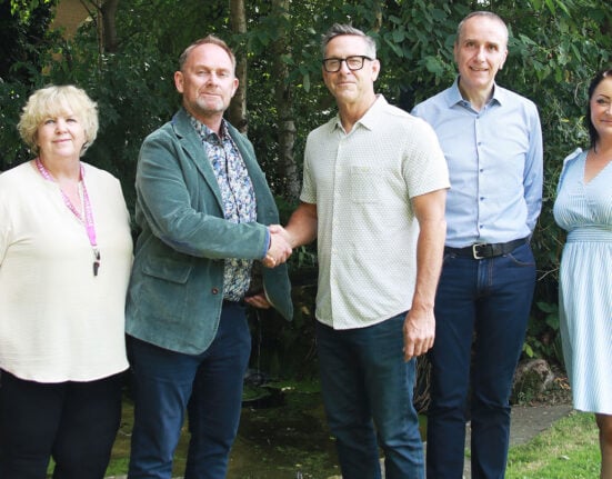
To spotlight these shifts, SEMI convened its first ‘Semiconductor Testing and Metrology in the AI Era: Industry Insights and Advocacy Press Conference’, hosted by Terry Tsao, Global Chief Marketing Officer and President of Taiwan, SEMI, with insights from I-Shih Tseng, CEO and President of Chroma ATE Inc. and Chair of the SEMI Inspection & Metrology Committee, and Gauss Chang, President of KYEC, along with more than 20 industry representatives.
SEMI surveyed companies across the semiconductor value chain, from IC design and fab manufacturing to testing services and test and metrology equipment. The findings revealed broad alignment on three priorities: dedicated policy, talent programmes, and shared advanced testing infrastructure. Respondents also called for testing and metrology to play a greater role in semiconductor policy, backed by stronger public-private collaboration to capture AI-driven opportunities.
As the industry enters its next growth phase, deeper value-chain collaboration will be essential. Through this initiative, SEMI is bringing industry voices together to align priorities, strengthen dialogue, and accelerate action, advancing the theme of SEMICON Taiwan 2026, ‘Transform Tomorrow’, ahead of the September exhibition.
Global test equipment surges as Taiwan metrology hits record high
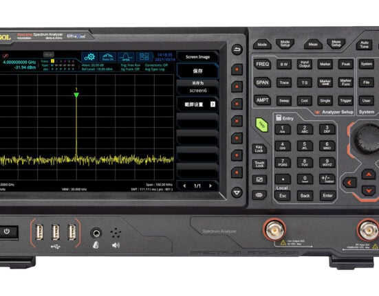
Testing and metrology are becoming critical growth engines as AI chips grow more complex. SEMI forecasts global semiconductor equipment sales to rise from $135 billion in 2025 to nearly $230 billion by 2028, with testing equipment surging 31% in 2026 to $15.3 billion and reaching $20.8 billion by 2028. Taiwan is seeing similar momentum. According to the latest data from the Department of Statistics, Ministry of Economic Affairs, Metrology industry output hit a record NT$193.6 billion last year, while output in the first five months of this year jumped 32.8% year over year, driven by rising test intensity for advanced logic, HBM, and HPC, and growing demand for memory testing, system-level testing (SLT), burn-in, and reliability screening.
World-class execution, industry eyes a greater role in global standards
Taiwan’s highly integrated semiconductor ecosystem gives testing and metrology companies a strong edge in collaboration, production efficiency, and speed. In the SEMI survey, respondents strongly recognised Taiwan’s competitiveness in close integration with fabs and OSATs (96.4%), testing efficiency and cost control (71.4%), and customisation and delivery flexibility (67.9%), reinforcing Taiwan’s position as a fast, integrated, and reliable semiconductor hub.
As AI accelerates industry growth, the next priority is moving up the technology value chain. The survey points to room for stronger R&D, proprietary technologies, and global standards participation, with 42.3% of respondents calling for government support to engage in international standards organisations. By strengthening these capabilities, Taiwan can evolve from a world-class supply chain partner into a contributor shaping the next generation of testing and metrology technologies and standards.
“As AI chips grow more complex and valuable, testing and metrology are no longer simply part of the manufacturing process. They are becoming a strategic capability that determines yield, cost, and speed to market,” said Terry Tsao, Global Chief Marketing Officer and President of Taiwan, SEMI. “Taiwan’s strengths in advanced manufacturing, packaging, and supply chain integration provide a powerful foundation. The next step is to turn that execution strength into greater technology leadership and global influence. SEMI will continue bringing industry and government together to strengthen the ecosystem and capture the next wave of AI-driven growth.”
Beyond quality control: system-level testing and silicon photonics take centre stage
AI is emerging as a key growth engine for testing and metrology, with more than 90% of SEMI survey respondents expecting AI-related business to grow over the next three years. As chip performance rises, so do demands for test speed and measurement precision.
Testing is also moving upstream: half of respondents say it should be integrated earlier into design-for-test (DFT) and design-for-manufacturability (DFM). Advanced packaging test for CoWoS and SoIC, and optoelectronic measurement for silicon photonics, rank as the industry’s top technology priorities.
“Testing and metrology were once viewed as end-of-line quality control. AI has made them mission-critical,” said I-Shih Tseng, CEO and President of Chroma ATE Inc. and Chair of the SEMI Inspection & Metrology Committee. “Without measurement, there is no validation, and without validation, no technology can scale. Taiwan’s next step is to strengthen the measurement and validation capabilities behind advanced technologies. Competitiveness is not just about what we can manufacture, but how precisely we can measure and control it. The SEMI Inspection & Metrology Committee will continue driving earlier integration of testing and metrology into design and R&D to support reliable AI innovation at scale.”
Talent gaps widen as cross-disciplinary expertise falls short
Talent emerged as the industry’s most urgent and widespread challenge in the SEMI survey. Every respondent reported some degree of talent shortage, while more than 60% ranked talent as the top priority among four major industry challenges. Optical metrology, cross-disciplinary system integration, and advanced packaging and testing were identified as the hardest roles to fill, underscoring a growing need for interdisciplinary talent development.
“Testing was once a supporting function; today, it is critical to semiconductor manufacturing,” said Gauss Chang, President of KYEC. “As advanced packaging and AI chips grow more complex and valuable, testing is no longer just about finding defects; it is about ensuring high-value chips can be delivered with confidence. With a single AI chip potentially worth tens of thousands of dollars, testing directly impacts yield, product value, and supply chain competitiveness. Closer industry-academia collaboration in talent and R&D will be essential to advancing the next generation of testing and metrology.”
Industry consensus coalesces around three policy priorities
The survey points to broad industry alignment around three priorities for policy support. First, establish a dedicated testing and metrology policy with targeted funding for technology R&D and equipment upgrades. Second, strengthen the talent pipeline through university curriculum reform and dedicated testing and metrology programs. Third, create shared advanced testing infrastructure to lower investment barriers, accelerate technology adoption, and strengthen industry competitiveness.
This momentum will continue at SEMICON Taiwan 2026. The Testing Pavilion will spotlight AI chips, advanced packaging, analog and mixed-signal IC, and memory testing, while the Advanced Testing Forum and Semiconductor Advanced Inspection and Metrology Forum will explore emerging technologies and cross-disciplinary collaboration. The Silicon Photonics Global Summit, 3DIC Global Summit, and Heterogeneous Integration Global Summit will further highlight key technologies shaping next-generation AI infrastructure.
SEMICON Taiwan 2026 begins with pre-show forums on 31st August, followed by the exhibition from 2-4th September at TaiNEX. Registration for the exhibition and forums is now open. Visit the official website for details and registration.