






Semiconductor equipment spending is entering a new growth cycle shaped by geopolitics, sovereignty strategies, and technology roadmaps, despite uneven end-market demand. Pressure on chipmaker profitability remains, with risks of overcapacity, fab redundancy, and low utilisation. However, WFE revenue is still expected to grow. Yole Group’s analysts announce a combination of market drivers, including higher equipment intensity across advanced logic, DRAM/HBM, NAND, and advanced packaging.
Against this backdrop, the market research & strategy consulting company releases its latest report, Status of the Wafer Fab Equipment Industry 2026, offering a comprehensive analysis of the market, technology, and supply chain trends shaping the industry’s future.
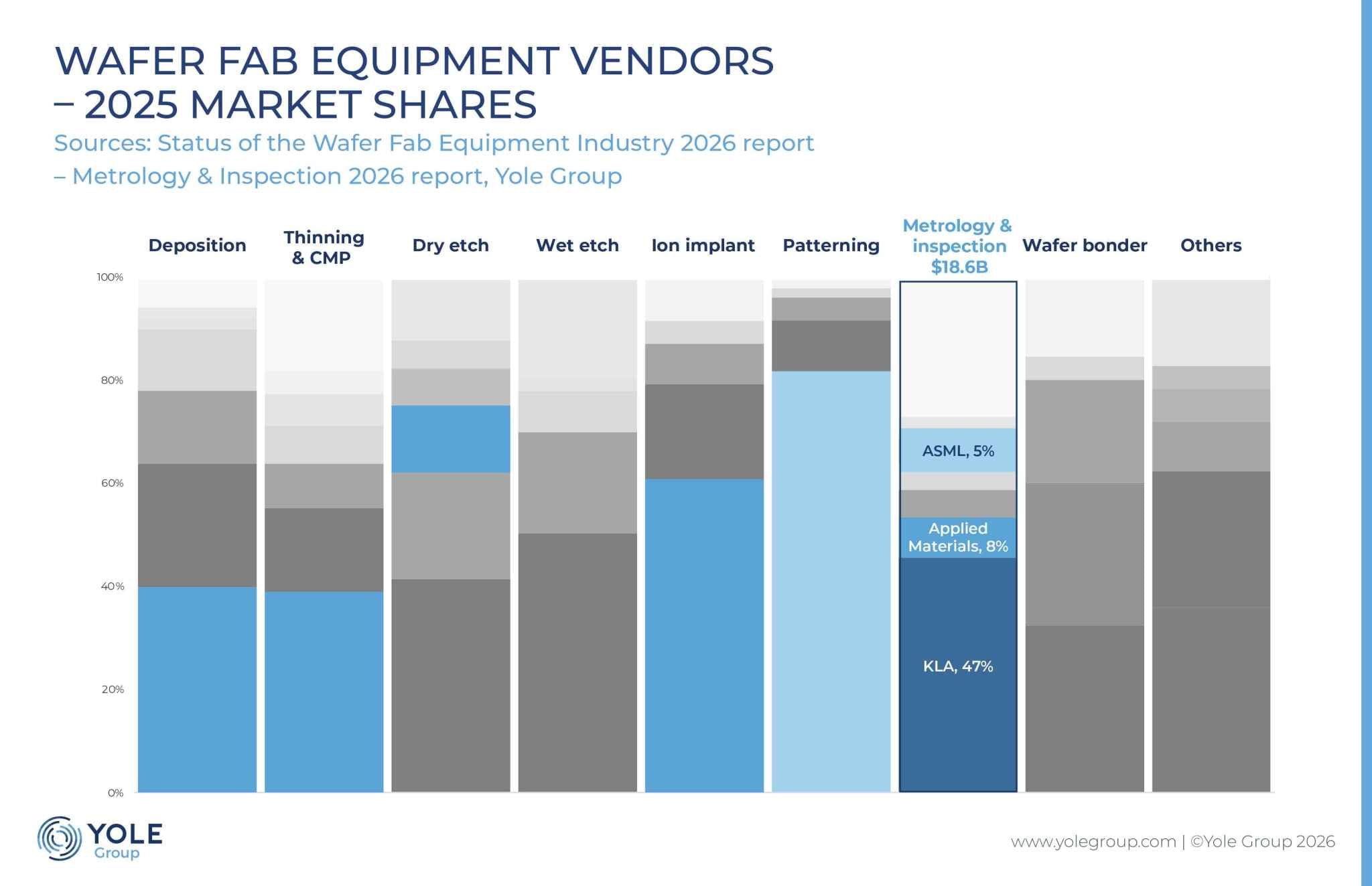
WFE sales revenue reached $129 billion in 2025 and is forecast to approach $220 billion by 2031, a 2025-2031 CAGR of 9%. Cumulative sales will exceed $1.2 trillion. This growth is underpinned by an expanding installed base, recurring service contracts, and increasingly complex fab automation requirements.
The market remains concentrated, with the top 5 WFE vendors, ASML, Applied Materials, Lam Research, Tokyo Electron, and KLA, together accounting for roughly 70% of revenue in 2025. This market structure reflects the high barriers to entry and long qualification cycles required to scale process-specific equipment into high-volume manufacturing. Even so, this concentration is increasingly challenged at the margins by Chinese vendors, whose progress is real but highly segment-dependent: strong in deposition, etch, and CMP, yet still negligible in lithography and metrology & inspection tools.
“Today one out of every three tools on the planet ships to China. The real question is no longer whether they buy; it’s how long before they no longer need to,” said Paule Durin PhD, Technology & Market Analyst, Semiconductor Equipment at Yole Group.
Segmented by equipment technology, patterning led the market at 27% of WFE in 2025 and is forecast to grow at a 10.9% CAGR to roughly $65 billion by 2031, a cumulative value of about $364.5 billion, driven by EUV and High-NA preparation.
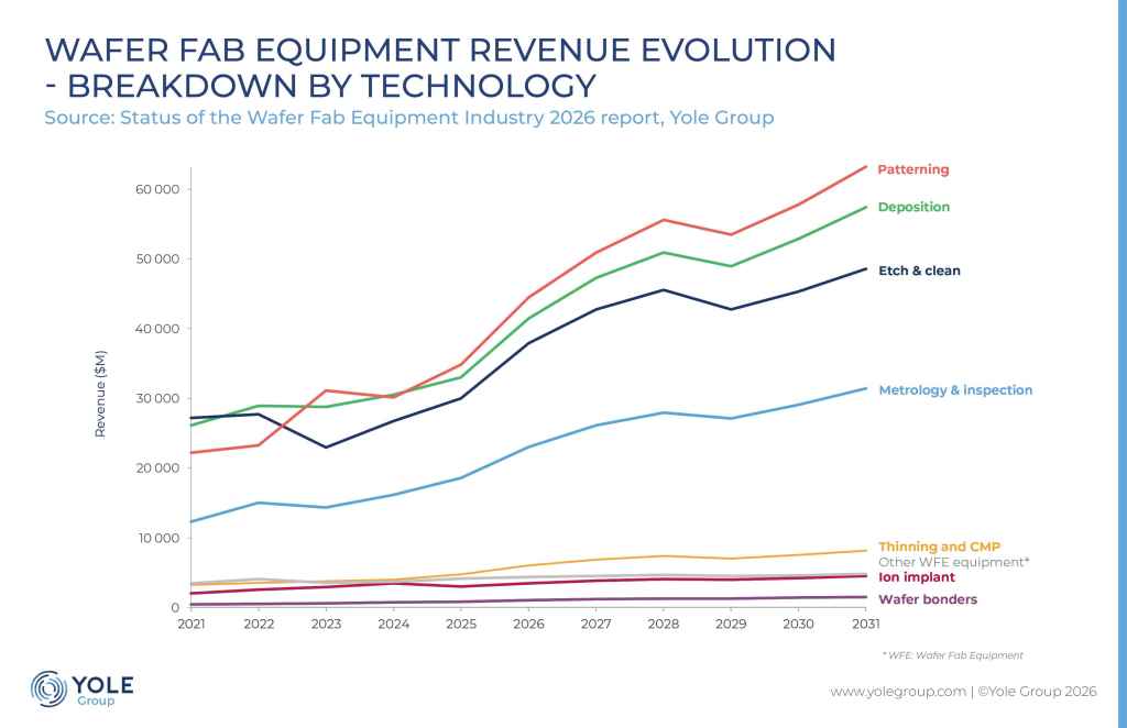
Deposition, 26% of WFE in 2025, is expected to grow at more than 9% CAGR, while etch & clean, 23% in 2025, grows at 8% CAGR. Metrology & inspection, 14% of WFE in 2025, is set to grow at 9.6% CAGR. And wafer bonding, though under 1% of the market in 2025, is forecast to outgrow the overall market with more than 10% CAGR to 2031.
“At the leading edge, complexity is the real growth driver: each move toward GAA and 3D stacking adds another layer to pattern, and another to inspect. Advanced packaging compounds this, as hybrid bonding and 3D stacks bury defects under opaque layers that optical tools cannot see through,” said Clara Grcevic, Technology & Market Analyst, Semiconductor Equipment at Yole Group.
By device application, advanced logic (less than 7nm) represented 27% of WFE revenue in 2025 and is expected to reach about 34% by 2031. This segment is becoming the market’s main growth engine, supported by GAA, higher EUV intensity, and backside power delivery. Advanced packaging, around 7% of WFE revenue in 2025, is forecast to rise to about 9% by 2031, supported by HBM, chiplets, hybrid bonding, and 2.5D/3D integration. This evolution is underlining the industry’s shift toward higher-value, more complex equipment.
With WFE revenue on track to nearly double by 2031, the pace and direction of this new growth cycle have never been more critical for equipment manufacturers, chipmakers, and investors. The Status of the Wafer Fab Equipment Industry 2026 report and Wafer Fab Equipment Market Monitor, both products from Yole Group, provide the market intelligence and technology insights required to navigate this rapidly evolving landscape and identify future growth opportunities.