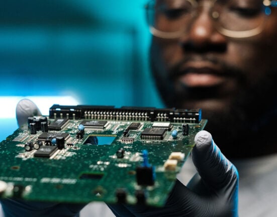






Materials science gives the semiconductor industry an essential tool for building supply chain resilience. Every chip starts as a stack of carefully engineered substances, from the elements in its substrate to the chemicals that define its circuits.
When chemists and materials engineers refine those substances, chipmakers can lean less on scarce suppliers and absorb disruptions at lower cost. Following a chip from raw material sourcing through fabrication, packaging, and end-of-life recovery reveals where that work strengthens each stage.
Raw materials behind semiconductor supply chains
Chipmakers face their first exposure long before a wafer enters a fab. Gallium demonstrates how that exposure builds from import through end use:
- Primary output: with no homegrown source of raw gallium, manufacturers in the United States depend on imported supply from Japan, Germany, Canada, and China to meet demand
- End use: integrated circuits account for most US gallium consumption
- Wafer form: the bulk of that supply takes the form of gallium arsenide, gallium nitride, and gallium phosphide wafers
Concentration at both ends turns the element into a structural chokepoint for semiconductor supply chains. When one supplier falters, device makers further down the line often feel the disruption.
Stockpiles, allied partnerships, and new onshore capacity help cushion those shocks. Policymakers and industry groups back all three as part of broader efforts to secure critical materials for chipmaking. Such measures buy time, but materials scientists working on substitutes, recycling, and domestic refining aim to cut import needs over the long term.
How materials science strengthens fabrication
Inside the fab, the problem for engineers shifts from supply to precision at the nanometer scale. Many in the industry credit extreme ultraviolet (EUV) lithography with keeping Moore’s Law on track because it prints the smallest chip features. Much of that success rests on the photoresist, a light-sensitive layer that records each circuit pattern when EUV light hits the wafer.
Because the coating’s formulation governs how accurately each feature forms, researchers often pair new chemistries with careful measurement throughout development. Ragged edges on a transistor gate can limit device performance and yield at leading-edge nodes. Cleaner patterns can help fabs pull more usable chips from each wafer, an efficiency gain that stretches scarce materials further.
Why packaging needs material precision
At the assembly stage, engineers prepare each die for years of heat cycling, so cleanliness shapes reliability as much as performance. Flip chip, heterogeneous integration, and fan-out wafer-level packaging rely on near-perfect contact surfaces, since microscopic films can disrupt conductive paths and thermal transfer over time.
Because these architectures squeeze more connections into less space, they leave little margin for error.
For example, residual material can weaken adhesion between layers and make a package more prone to delamination. One plasma cleaning method strips nanoscale organic contamination from bonding surfaces, and its design suits a busy production line:
- In-line operation: the dry process treats parts continuously as they move through production, with no batch queuing
- Vacuum-free design: cleaning runs at atmospheric pressure
- High-volume compatibility: its minimal impact on line balance keeps output moving
As one tool among many, plasma cleaning illustrates why production teams aim to remove surface films before they lead to rework or field failures. Clean bonds help protect everything invested upstream, from refined gallium to patterned wafers, and carry that value through a chip’s years in service.
Materials recovery and circularity
Resilience also depends on what recyclers can pull from a retired laptop or a decommissioned solar farm. Those devices contain critical materials that semiconductors rely on, including gallium, indium, and rare earth elements.
Reclaiming that content could give chipmakers a second supply stream and ease pressure on imports. Research teams working on recovering critical materials from e-waste have developed promising laboratory techniques, though the leap to industrial volumes is still ahead. Pilot plants need to prove that new separation and extraction chemistries can hold up at scale.
If those efforts pay off, recovery becomes the final link in a materials-driven approach to resilience, returning discarded electronics to the supply chain’s starting point.
Materials science powers future resilience
Chipmakers build security one step at a time. Substitution research and recycling expands supply of critical materials. Better resists and cleaner bonding surfaces make that supply go further, because fewer chips fail along the way.
Those innovations come from chemists, engineers, and recyclers attacking the same scarcity problem from different directions. Sustained investment in materials science across sourcing, fabrication, packaging, and recovery will largely shape how resilient the chip supply chain becomes.