As semiconductor devices become increasingly complex, metrology and inspection are evolving from manufacturing support functions into strategic enablers of semiconductor innovation. Driven by AI, advanced packaging, HBM, and next-generation architectures, process-control requirements are rising faster than ever across the industry.
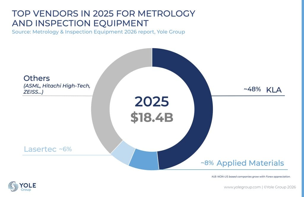
According to Yole Group’s analysis, the metrology & inspection equipment market reached more than $18 billion in 2025, representing approximately 14% of total wafer fab equipment spending. The market is expected to grow to about $25 billion by 2031. This growth reflects both cyclical recovery and a structural increase in process-control intensity driven by advanced architectures, AI-related demand, and the growing importance of advanced packaging.
“As AI, HBM, and advanced packaging push semiconductor complexity to new levels, metrology and inspection are becoming critical differentiators for yield, performance, and time-to-market,” said Clara Grcevic, Technology & Market Analyst, Semiconductor Equipment, at Yole Group.
Yole Group’s report explores how the industry is transitioning from traditional 2D scaling toward a new era defined by 3D integration, buried structures, hybrid bonding, and heterogeneous packaging. New semiconductor architectures such as Gate-All-Around (GAA), backside power delivery networks, taller 3D NAND stacks, and future memory innovations are creating measurement and inspection challenges that conventional approaches can no longer address on their own.
One of the key findings of the report is the growing importance of advanced packaging and HBM. The rapid deployment of AI infrastructure is accelerating demand for these technologies, further increasing process-control intensity across the semiconductor manufacturing flow. As chiplet architectures, hybrid bonding, and increasingly complex package designs become mainstream, manufacturers face new yield risks associated with warpage, alignment accuracy, voids, delamination, and buried defects. As a result, process control is becoming a critical differentiator throughout the packaging flow.
Yole Group’s analysts also highlight an evolving competitive landscape. While established leaders, KLA, Applied Materials, and Lasertec continue to dominate the market, competition is increasingly expanding toward software, analytics, hybrid metrology, and application-specific process-control solutions.
“Advanced packaging, hybrid bonding and High-NA EUV challenges are redefining process-control requirements and creating attractive growth opportunities in the metrology & inspection market,” comments Clara Grcevic from Yole Group.
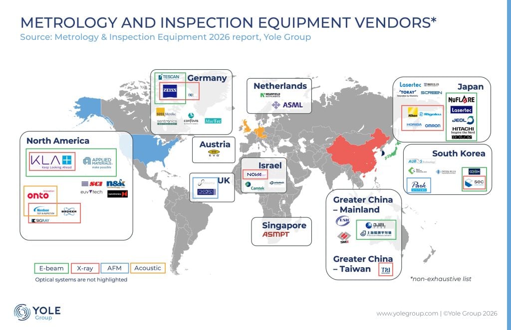
Moreover, the strongest growth between 2024 and 2025 came from companies exposed to the most dynamic process-control demand segments. ASML and ZEISS benefited from continued EUV adoption and rising demand for mask and optics metrology, while Hitachi High-Tech and Nova were supported by increasing process-control intensity in leading-edge logic and memory. Skyverse, from a smaller base, likely reflects the impact of China’s localization momentum.
In addition, this report examines the growing impact of geopolitics and localisation strategies, particularly in China. Export controls, domestic equipment requirements, and regional policy initiatives are creating a more fragmented market environment, while simultaneously accelerating the development of local ecosystems.
As semiconductor innovation shifts toward 3D architectures, advanced packaging, and AI-driven systems, process control is becoming a strategic differentiator across the value chain. Understanding how metrology and inspection technologies evolve will be essential for anticipating future manufacturing challenges and capturing emerging growth opportunities.


